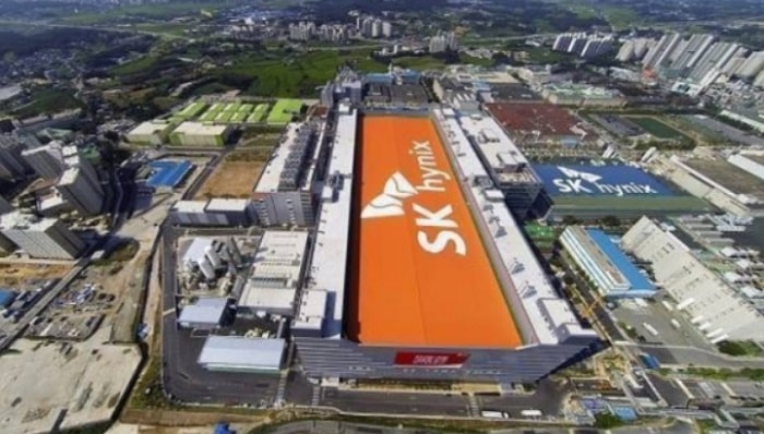
SK Hynix Inc., the world’s leading high bandwidth memory (HBM) chip producer, will plow in $3.87 billion to build advanced packaging and research and development facilities for AI chips in Indiana, which would be the first of its kind in the US and the company’s first overseas HBM chip plant.
According to a press release by SK Hynix on Thursday, the South Korean chip giant signed an investment agreement the day before with the State of Indiana, Purdue University and the US government to build advanced chip packaging and R&D facilities in West Lafayette, Indiana with an investment of $3.87 billion.
At the plant, the company will produce HBM chips and leverage talent from Purdue University, also in West Layfayette, famous for its strong semiconductor and hardware AI R&D capabilities and experts, to develop next-generation chip technology.
The company aims to start mass-producing the high-performance, high-value memory chips, essential components in running graphics processing units (GPU) that train AI systems like ChatGPT, in the second half of 2028.
This marks the first attempt to build an advanced packaging facility for AI chips in the US. It is also the company’s first-ever US chip plant and first HBM-producing facility abroad.
“We are excited to become the first in the industry to build a state-of-the-art advanced packaging facility for AI products in the United States that will help strengthen supply-chain resilience and develop a local semiconductor ecosystem,” SK Hynix Chief Executive Officer Kwak Noh-Jung said at an agreement signing ceremony.
“With this new facility, we hope to advance our goal of providing AI memory chips with unmatched capabilities, serving the needs of our customers.”
SK Hynix commands the global HBM chip market with about 50% share, ahead of its bigger memory rival Samsung Electronics Co., according to TrendForce. In the latest-generation HBM3 market, SK Hynix holds over 90% share.


